 | –≠–ª–µ–∫—Ç—Ä–æ–Ω–Ω—ã–π –∫–æ–º–ø–æ–Ω–µ–Ω—Ç: SP506 | –°–∫–∞—á–∞—Ç—å:  PDF PDF  ZIP ZIP |
1
Rev: A Date: 1/27/04
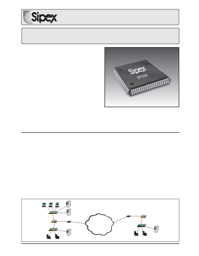
SP506 Multi≠Mode Serial Transceiver
© Copyright 2004 Sipex Corporation
The SP506 is a monolithic IC that supports eight (8) popular serial interface standards for DTE
to DCE connectivity. The SP506 is pin-to-pin compatible to our SP505 multi-protocol transceiver
but with faster throughput. The seven (7) drivers and seven (7) receivers can transmit and receive
signals at 20Mbps. As with the SP505, the SP506 requires no additional external components
for compliant operation for all of the eight (8) modes of operation. All necessary termination is
integrated within the SP506 and is switchable when V.35 drivers, V.35 receivers, and V.11
receivers are used. The SP506 can operate as either a DTE or DCE.
Additional features with the SP506 include internal loopback that can be initiated in either single-
ended or differential modes. While in loopback mode, driver outputs are internally connected to
receiver inputs creating an internal signal path convenient for diagnostic testing. This eliminates
the need for an external loopback plug. The SP506 also includes a latch enable pin with the driver
and receiver address decoder. Tri-state ability for the driver and receiver outputs is controlled by
supplying a 4-bit word into the address decoder. Seven (7) drivers and one (1) receiver in the
SP506 include separate enable pins for added convenience.
SP506
5V, Single Chip WAN Multi-Mode Serial Transceiver
DESCRIPTION
Interface Modes Supported:
RS-232
(V.28)
X.21/RS-422
(V.11)
EIA-530
(V.10 & V.11)
EIA-530A
(V.10 & V.11)
RS-449
(V.10 & V.11)
V.35
(V.35 & V.28)
V.36
(V.10 & V.11)
RS-485
(unterminated V.11)
Software Selectable Protocol
Highest Differential Transmission Rates
at over 20Mbps
+5V Only Operation
Seven (7) Drivers and Seven (7) Receivers
Driver and Receiver Tri-state Control
Internal Transceiver Termination Resistors for
V.11 and V.35 Protocols
Loopback Self-Test Mode
Improved ESD Tolerance for Analog I/Os
Compliant to NET1/2 and TBR2 Physical Layer
Requirements
Used in WAN Serial Ports in Routers, Switches,
DSU/CSU's and other Access Devices
EIA-530
WAN
V.35
Æ

2
Rev: A Date: 1/27/04
SP506 Multi≠Mode Serial Transceiver
© Copyright 2004 Sipex Corporation
SPECIFICATIONS
T
A
= +25∞C and V
CC
= +4.75V to +5.25V unless otherwise noted.
MIN.
TYP.
MAX.
UNITS
CONDITIONS
LOGIC INPUTS
V
IL
0.8
Volts
V
IH
2.0
Volts
LOGIC OUTPUTS
V
OL
0.4
Volts
I
OUT
= ≠3.2mA
V
OH
2.4
Volts
I
OUT
= 1.0mA
V.28 DRIVER
DC Parameters
Outputs
Open Circuit Voltage
±15
Volts
per Figure 1
Loaded Voltage
±5.0
±15
Volts
per Figure 2
Short-Circuit Current
±100
mA
per Figure 4
Power-Off Impedance
300
per Figure 5
AC Parameters
V
CC
= +5V for AC parameters
Outputs
Transition Time
1.5
µ
s
per Figure 6; +3V to -3V
Instantaneous Slew Rate
30
V/
µ
s
per Figure 3
Propagation Delay
t
PHL
0.5
1
5
µ
s
t
PLH
0.5
1
5
µ
s
Max.Transmission Rate
120
230
kbps
V.28 RECEIVER
DC Parameters
Inputs
Input Impedance
3
7
k
per Figure 7
Open-Circuit Bias
+2.0
Volts
per Figure 8
HIGH Threshold
1.7
3.0
Volts
LOW Threshold
0.8
1.2
Volts
AC Parameters
V
CC
= +5V for AC parameters
Propagation Delay
t
PHL
50
100
500
ns
t
PLH
50
100
500
ns
ABSOLUTE MAXIMUM RATINGS
These are stress ratings only and functional operation
of the device at these ratings or any other above those
indicated in the operation sections of the specifications
below is not implied. Exposure to absolute maximum
rating conditions for extended periods of time may
affect reliability.
V
CC
............................................................................+7V
Input Voltages:
Logic...............................-0.3V to (V
CC
+0.5V)
Drivers............................-0.3V to (V
CC
+0.5V)
Receivers........................................±15.5V
Output Voltages:
Logic................................-0.3V to (V
CC
+0.5V)
Drivers................................................±15V
Receivers........................-0.3V to (V
CC
+0.5V)
Storage Temperature..........................-65∞C to +150∞C
Power Dissipation per package
80-pin QFP (derate 18.3mW/∞C above +70
o
C)...1500mW
STORAGE CONSIDERATIONS
Due to the relatively large package size of the 80-pin
quad flat-pack, storage in a low humidity environment
is preferred. Large high density plastic packages are
moisture sensitive and should be stored in Dry Vapor
Barrier Bags. Prior to usage, the parts should remain
bagged and stored below 40∞C and 60%RH. If the parts
are removed from the bag, they should be used within
48 hours or stored in an environment at or below 20%RH.
If the above conditions cannot be followed, the parts
should be baked for four hours at 125∞C in order
remove moisture prior to soldering. Sipex ships the
80-pin QFP in Dry Vapor Barrier Bags with a humidity
indicator card and desiccant pack. The humidity indicator
should be below 30%RH.

3
Rev: A Date: 1/27/04
SP506 Multi≠Mode Serial Transceiver
© Copyright 2004 Sipex Corporation
SPECIFICATIONS
T
A
= +25∞C and V
CC
= +4.75V to +5.25V unless otherwise noted.
MIN.
TYP.
MAX.
UNITS
CONDITIONS
V.28 RECEIVER (continued)
AC Parameters (cont.)
Max.Transmission Rate
120
230
kbps
V.10 DRIVER
DC Parameters
Outputs
Open Circuit Voltage
±4.0
±6.0
Volts
per Figure 9
Test-Terminated Voltage
0.9V
OC
Volts
per Figure 10
Short-Circuit Current
±150
mA
per Figure 11
Power-Off Current
±100
µ
A
per Figure 12
AC Parameters
V
CC
= +5V for AC parameters
Outputs
Transition Time
200
ns
per Figure 13; 10% to 90%
Propagation Delay
t
PHL
50
100
500
ns
t
PLH
50
100
500
ns
Max.Transmission Rate
120
kbps
V.10 RECEIVER
DC Parameters
Inputs
Input Current
≠3.25
+3.25
mA
per Figures 14 and 15
Input Impedance
4
k
Sensitivity
±0.3
Volts
AC Parameters
V
CC
= +5V for AC parameters
Propagation Delay
t
PHL
50
120
250
ns
t
PLH
50
120
250
ns
Max.Transmission Rate
120
kbps
V.11 DRIVER
DC Parameters
Outputs
Open Circuit Voltage
±5.0
Volts
per Figure 16
Test Terminated Voltage
±2.0
Volts
per Figure 17
0.5V
OC
0.67V
OC
Volts
Balance
±0.4
Volts
per Figure 17
Offset
+3.0
Volts
per Figure 17
Short-Circuit Current
±150
mA
per Figure 18
Power-Off Current
±100
µ
A
per Figure 19
AC Parameters
V
CC
= +5V for AC parameters
Outputs
Transition Time
20
ns
per Figures 21 and 36; 10% to 90%
Propagation Delay
t
PHL
50
65
85
ns
per Figures 33 and 36, C
L
= 50pF
t
PLH
50
65
85
ns
per Figures 33 and 36, C
L
= 50pF
Differential Skew
10
20
ns
per Figures 33 and 36, C
L
= 50pF
Max.Transmission Rate
20
Mbps
per Figure 33, C
L
= 50pF
f
IN
= 10MHz
V.11 RECEIVER
DC Parameters
Inputs
Common Mode Range
≠7
+7
Volts
Sensitivity
±0.3
Volts

4
Rev: A Date: 1/27/04
SP506 Multi≠Mode Serial Transceiver
© Copyright 2004 Sipex Corporation
SPECIFICATIONS
T
A
= +25∞C and V
CC
= +4.75V to +5.25V unless otherwise noted.
MIN.
TYP.
MAX.
UNITS
CONDITIONS
V.11 RECEIVER (continued)
DC Parameters (cont.)
Input Current
≠3.25
±3.25
mA
per Figure 20 and 22
Current w/ 100 Termination
±60.75
mA
per Figure 23 and 24
Input Impedance
4
k
AC Parameters
V
CC
= +5V for AC parameters
Propagation Delay
t
PHL
30
65
85
ns
per Figures 33 and 38; C
L
= 50pF
t
PLH
30
65
85
ns
per Figures 33 and 38; C
L
= 50pF
Differential Skew
10
ns
per Figure 33; C
L
= 50pF
Max.Transmission Rate
20
Mbps
per Figure 33; C
L
= 50pF
f
IN
= 10MHz
V.35 DRIVER
DC Parameters
Outputs
Open Circuit Voltage
±1.20
Volts
per Figure 16
Test Terminated Voltage
±0.44
±0.66
Volts
per Figure 25
Offset
±0.6
Volts
per Figure 25
Source Impedance
50
150
per Figure 27; Z
S
= V
2
/V
1
x 50
Short-Circuit Impedance
135
165
per Figure 28
AC Parameters
V
CC
= +5V for AC parameters
Outputs
Transition Time
30
40
ns
per Figure 29; 10% to 90%
Propagation Delay
t
PHL
50
70
90
ns
per Figures 33 and 36; C
L
= 20pF
t
PLH
50
70
90
ns
per Figures 33 and 36; C
L
= 20pF
Differential Skew
7
10
ns
per Figures 33 and 36; C
L
= 20pF
Max.Transmission Rate
20
Mbps
per Figure 33; C
L
= 20pF
f
IN
= 10MHz
V.35 RECEIVER
DC Parameters
Inputs
Sensitivity
±80
mV
Source Impedance
90
110
per Figure 30; Z
S
= V
2
/V
1
x 50
Short-Circuit Impedance
135
165
per Figure 31
AC Parameters
V
CC
= +5V for AC parameters
Propagation Delay
t
PHL
30
75
90
ns
per Figures 33 and 38; C
L
= 20pF
t
PLH
30
75
90
ns
per Figures 33 and 38; C
L
= 20pF
Differential Skew
10
ns
per Figure 33; C
L
= 20pF
Max.Transmission Rate
20
Mbps
per Figure 33; C
L
= 20pF
f
IN
= 10MHz
TRANSCEIVER LEAKAGE CURRENTS
Driver Output 3-State Current
500
µ
A
per Figure 32; Drivers disabled
Rcvr Output 3-State Current
1
10
µ
A
DEC
X
= 0000, 0.4V V
O
2.4V

5
Rev: A Date: 1/27/04
SP506 Multi≠Mode Serial Transceiver
© Copyright 2004 Sipex Corporation
OTHER AC CHARACTERISTICS
T
A
= +25∞C and V
CC
= +5.0V unless otherwise noted.
PARAMETER
MIN.
TYP.
MAX.
UNITS
CONDITIONS
DRIVER DELAY TIME BETWEEN ACTIVE MODE AND TRI-STATE MODE
RS-232/V.28
t
PZL
; Tri-state to Output LOW
0.70
5.0
µ
s
C
L
= 100pF, Fig. 34 & 40; S
1
closed
t
PZH
; Tri-state to Output HIGH
0.40
2.0
µ
s
C
L
= 100pF, Fig. 34 & 40; S
2
closed
t
PLZ
; Output LOW to Tri-state
0.20
2.0
µ
s
C
L
= 100pF, Fig. 34 & 40; S
1
closed
t
PHZ
; Output HIGH to Tri-state
0.40
2.0
µ
s
C
L
= 100pF, Fig. 34 & 40; S
2
closed
RS-423/V.10
t
PZL
; Tri-state to Output LOW
0.15
2.0
µ
s
C
L
= 100pF, Fig. 34 & 40; S
1
closed
t
PZH
; Tri-state to Output HIGH
0.20
2.0
µ
s
C
L
= 100pF, Fig. 34 & 40; S
2
closed
t
PLZ
; Output LOW to Tri-state
0.20
2.0
µ
s
C
L
= 100pF, Fig. 34 & 40; S
1
closed
t
PHZ
; Output HIGH to Tri-state
0.15
2.0
µ
s
C
L
= 100pF, Fig. 34 & 40; S
2
closed
RS-422/V.11
t
PZL
; Tri-state to Output LOW
2.80
10.0
µ
s
C
L
= 100pF, Fig. 34 & 37; S
1
closed
t
PZH
; Tri-state to Output HIGH
0.10
2.0
µ
s
C
L
= 100pF, Fig. 34 & 37; S
2
closed
t
PLZ
; Output LOW to Tri-state
0.10
2.0
µ
s
C
L
= 15pF, Fig. 34 & 37; S
1
closed
t
PHZ
; Output HIGH to Tri-state
0.10
2.0
µ
s
C
L
= 15pF, Fig. 34 & 37; S
2
closed
V.35
t
PZL
; Tri-state to Output LOW
2.60
10.0
µ
s
C
L
= 100pF, Fig. 34 & 37; S
1
closed
t
PZH
; Tri-state to Output HIGH
0.10
2.0
µ
s
C
L
= 100pF, Fig. 34 & 37; S
2
closed
t
PLZ
; Output LOW to Tri-state
0.10
2.0
µ
s
C
L
= 15pF, Fig. 34 & 37; S
1
closed
t
PHZ
; Output HIGH to Tri-state
0.15
2.0
µ
s
C
L
= 15pF, Fig. 34 & 37; S
2
closed
RECEIVER DELAY TIME BETWEEN ACTIVE MODE AND TRI-STATE MODE
RS-232/V.28
t
PZL
; Tri-state to Output LOW
0.12
2.0
µ
s
C
L
= 100pF, Fig. 35 & 38; S
1
closed
t
PZH
; Tri-state to Output HIGH
0.10
2.0
µ
s
C
L
= 100pF, Fig. 35 & 38; S
2
closed
t
PLZ
; Output LOW to Tri-state
0.10
2.0
µ
s
C
L
= 100pF, Fig. 35 & 38; S
1
closed
t
PHZ
; Output HIGH to Tri-state
0.10
2.0
µ
s
C
L
= 100pF, Fig. 35 & 38; S
2
closed
RS-423/V.10
t
PZL
; Tri-state to Output LOW
0.10
2.0
µ
s
C
L
= 100pF, Fig. 35 & 38; S
1
closed
t
PZH
; Tri-state to Output HIGH
0.10
2.0
µ
s
C
L
= 100pF, Fig. 35 & 38; S
2
closed
t
PLZ
; Output LOW to Tri-state
0.10
2.0
µ
s
C
L
= 100pF, Fig. 35 & 38; S
1
closed
t
PHZ
; Output HIGH to Tri-state
0.10
2.0
µ
s
C
L
= 100pF, Fig. 35 & 38; S
2
closed

6
Rev: A Date: 1/27/04
SP506 Multi≠Mode Serial Transceiver
© Copyright 2004 Sipex Corporation
OTHER AC CHARACTERISTICS
(Continued)
T
A
= +25∞C and V
CC
= +5.0V unless otherwise noted.
PARAMETER
MIN.
TYP.
MAX.
UNITS
CONDITIONS
POWER REQUIREMENTS
PARAMETER
MIN.
TYP.
MAX.
UNITS
CONDITIONS
V
CC
4.75
5.00
5.25
Volts
I
CC
(No Mode Selected)
30
mA
All I
CC
values are with V
CC
= +5V
(V.28/RS-232)
65
mA
f
IN
= 120kbps; Drivers active & loaded.
(V.11/X.21)
175
mA
f
IN
= 10Mbps; Drivers active & loaded.
(EIA-530 & RS-449)
250
mA
f
IN
= 10Mbps; Drivers active & loaded.
(V.35)
100
mA
V.35 @ f
IN
= 10Mbps, V.28 @ 20kbps;
Drivers active & loaded.
RS-422/V.11
t
PZL
; Tri-state to Output LOW
0.10
2.0
µ
s
C
L
= 100pF, Fig. 35 & 39; S
1
closed
t
PZH
; Tri-state to Output HIGH
0.10
2.0
µ
s
C
L
= 100pF, Fig. 35 & 39; S
2
closed
t
PLZ
; Output LOW to Tri-state
0.10
2.0
µ
s
C
L
= 15pF, Fig. 35 & 39; S
1
closed
t
PHZ
; Output HIGH to Tri-state
0.10
2.0
µ
s
C
L
= 15pF, Fig. 35 & 39; S
2
closed
V.35
t
PZL
; Tri-state to Output LOW
0.10
2.0
µ
s
C
L
= 100pF, Fig. 35 & 39; S
1
closed
t
PZH
; Tri-state to Output HIGH
0.10
2.0
µ
s
C
L
= 100pF, Fig. 35 & 39; S
2
closed
t
PLZ
; Output LOW to Tri-state
0.10
2.0
µ
s
C
L
= 15pF, Fig. 35 & 39; S
1
closed
t
PHZ
; Output HIGH to Tri-state
0.10
2.0
µ
s
C
L
= 15pF, Fig. 35 & 39; S
2
closed
TRANSCEIVER TO TRANSCEIVER SKEW
(per Figures 33, 36, 38)
V.28 Driver
100
ns
[ (t
phl
)
Tx1
≠ (t
phl
)
Tx6,7
]
100
ns
[ (t
plh
)
Tx1
≠ (t
plh
)
Tx6,7
]
V.28 Receiver
20
ns
[ (t
phl
)
Rx1
≠ (t
phl
)
Rx2,7
]
20
ns
[ (t
plh
)
Rx1
≠ (t
phl
)
Rx2,7
]
V.11 Driver
2
ns
[ (t
phl
)
Tx1
≠ (t
phl
)
Tx6,7
]
2
ns
[ (t
plh
)
Tx1
≠ (t
plh
)
Tx6,7
]
V.11 Receiver
3
ns
[ (t
phl
)
Rx1
≠ (t
phl
)
Rx2,7
]
3
ns
[ (t
plh
)
Rx1
≠ (t
phl
)
Rx2,7
]
V.10 Driver
5
ns
[ (t
phl
)
Tx2
≠ (t
phl
)
Tx3,4,5
]
5
ns
[ (t
plh
)
Tx2
≠ (t
plh
)
Tx3,4,5
]
V.10 Receiver
5
ns
[ (t
phl
)
Rx2
≠ (t
phl
)
Rx3,4,5
]
5
ns
[ (t
plh
)
Rx2
≠ (t
phl
)
Rx3,4,5
]
V.35 Driver
4
ns
[ (t
phl
)
Tx1
≠ (t
phl
)
Tx6,7
]
4
ns
[ (t
plh
)
Tx1
≠ (t
plh
)
Tx6,7
]
V.35 Receiver
6
ns
[ (t
phl
)
Rx1
≠ (t
phl
)
Rx2,7
]
6
ns
[ (t
plh
)
Rx1
≠ (t
phl
)
Rx2,7
]
7
Rev: A Date: 1/27/04
SP506 Multi≠Mode Serial Transceiver
© Copyright 2004 Sipex Corporation
A
V
OC
C
A
V
T
C
3k
A
V
T
C
7k
Oscilloscope
Scope used for slew rate
measurement.
A
I
sc
C
A
C
V
CC
= 0V
±
2V
I
x
A
C
3k
2500pF
Oscilloscope
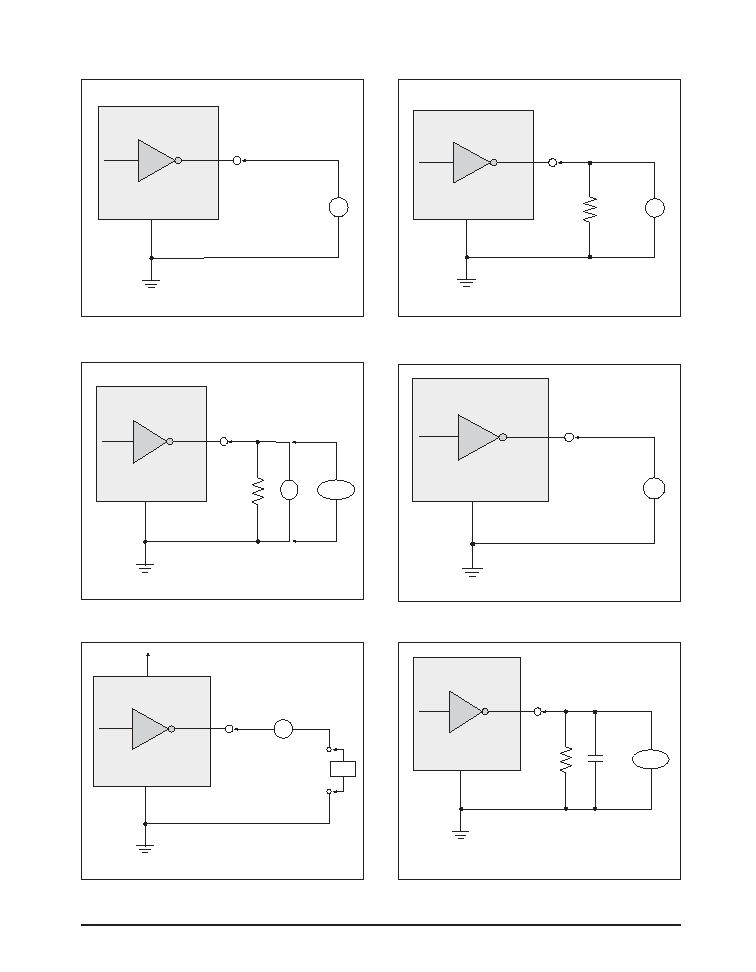
Figure 1. V.28 Driver Output Open Circuit Voltage
Figure 2. V.28 Driver Output Loaded Voltage
Figure 3. V.28 Driver Output Slew Rate
Figure 4. V.28 Driver Output Short-Circuit Current
Figure 6. V.28 Driver Output Rise/Fall Times
Figure 5. V.28 Driver Output Power-Off Impedance
TEST CIRCUITS

8
Rev: A Date: 1/27/04
SP506 Multi≠Mode Serial Transceiver
© Copyright 2004 Sipex Corporation
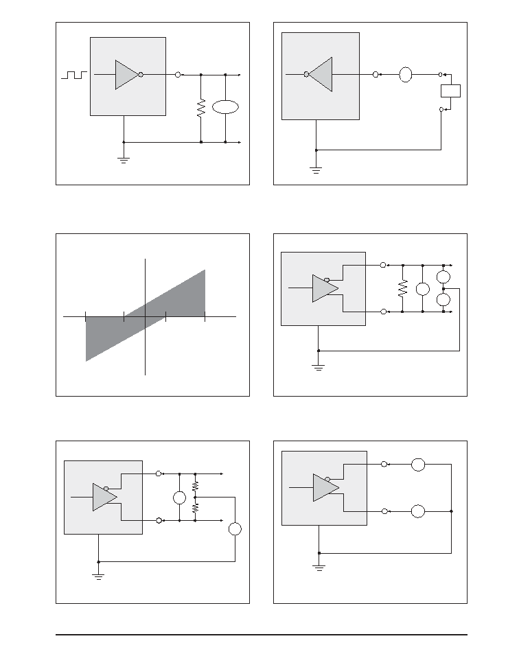
Figure 7. V.28 Receiver Input Impedance
A
C
I
ia
±
15V
A
C
V
oc
Figure 8. V.28 Receiver Input Open Circuit Bias
A
V
OC
3.9k
C
A
V
t
450
C
A
C
±
0.25V
V
CC
= 0V
I
x
A
I
sc
C
Figure 9. V.10 Driver Output Open-Circuit Voltage
Figure 10. V.10 Driver Output Test Terminated Voltage
Figure 12. V.10 Driver Output Power-Off Current
Figure 11. V.10 Driver Output Short-Circuit Current
9
Rev: A Date: 1/27/04
SP506 Multi≠Mode Serial Transceiver
© Copyright 2004 Sipex Corporation
Figure 13. V.10 Driver Output Transition Time
Figure 14. V.10 Receiver Input Current
A
450
C
Oscilloscope
A
C
I
ia
±
10V
+3.25mA
≠3.25mA
+10V
+3V
≠3V
≠10V
Maximum Input Current
versus Voltage
V.10 RECEIVER
Figure 15. V.10 Receiver Input IV Graph
Figure 16. V.11 and V.35 Driver Output Open-Circuit
Voltage
A
B
V
OC
3.9k
V
OCA
V
OCB
C
A
B
V
T
50
V
OS
C
50
A
B
C
I
sa
I
sb
Figure 17. V.11 Driver Output Test Terminated Voltage
Figure 18. V.11 Driver Output Short-Circuit Current

10
Rev: A Date: 1/27/04
SP506 Multi≠Mode Serial Transceiver
© Copyright 2004 Sipex Corporation
A
B
C
I
xa
±
0.25V
A
B
C
I
xb
±
0.25V
V
CC
= 0V
V
CC
= 0V
A
B
C
I
ia
±
10V
C
I
ib
±
10V
A
B
+3.25mA
≠3.25mA
+10V
+3V
≠3V
≠10V
Maximum Input Current
versus Voltage
V.11 RECEIVER
Figure 19. V.11 Driver Output Power-Off Current
Figure 20. V.11 Receiver Input Current
Figure 21. V.11 Driver Output Rise/Fall Time
Figure 22. V.11 Receiver Input IV Graph
A
B
50
C
50
50
V
E
Oscilloscope

11
Rev: A Date: 1/27/04
SP506 Multi≠Mode Serial Transceiver
© Copyright 2004 Sipex Corporation
A
B
C
I
ia
±
6V
C
I
ib
±
6V
A
B
100
to
150
100
to
150
i [mA] = V [V] / 0.1
+6V
+3V
≠3V
≠6V
Maximum Input Current
versus Voltage
V.11 RECEIVER
w/ Optional Cable Termination
(100
to 150
)
i [mA] = V [V] / 0.1
i [mA] = (V [V] ≠ 3) / 4.0
i [mA] = (V [V] ≠ 3) / 4.0
Figure 23. V.11 Receiver Input Current w/ Termination
Figure 24. V.11 Receiver Input Graph w/ Termination
Figure 25. V.35 Driver Output Test Terminated Voltage
Figure 26. V.35 Driver Output Offset Voltage
Figure 27. V.35 Driver Output Source Impedance
A
B
50
C
50
V
T
V
OS
A
B
V
2
50
C
24kHz, 550mV
p-p
Sine Wave
V
1
A
B
50
C
50
V
T
V
OS
12
Rev: A Date: 1/27/04
SP506 Multi≠Mode Serial Transceiver
© Copyright 2004 Sipex Corporation
Figure 32. Driver Output Leakage Current Test
Figure 33. Driver/Receiver Timing Test Circuit
Figure 30. V.35 Receiver Input Source Impedance
Figure 29. V.35 Driver Output Rise/Fall Time
Figure 31. V.35 Receiver Input Short-Circuit Impedance
Figure 28. V.35 Driver Output Short-Circuit Impedance
A
B
C
I
SC
±
2V
A
B
C
50
Oscilloscope
50
50
A
B
C
I
sc
±
2V
C
L1
15pF
R
OUT
A
B
A
B
T
IN
C
L2
f
IN
(50% Duty Cycle, 2.5V
P-P
)
A
B
V
2
50
C
24kHz, 550mV
p-p
Sine Wave
V
1
A
B
I
ZSC
Logic "1"
±
15V
0
0
0
0
DEC
3
DEC
2
DEC
1
DEC
0
V
CC
= 0V
V
CC
Any one of the three conditions for disabling the driver.

13
Rev: A Date: 1/27/04
SP506 Multi≠Mode Serial Transceiver
© Copyright 2004 Sipex Corporation
Figure 34. Driver Timing Test Load Circuit
Figure 35. Receiver Timing Test Load Circuit
500
C
L
Output
Under
Test
S
1
S
2
V
CC
1K
1K
C
RL
Receiver
Output
S
1
S
2
Test Point
V
CC
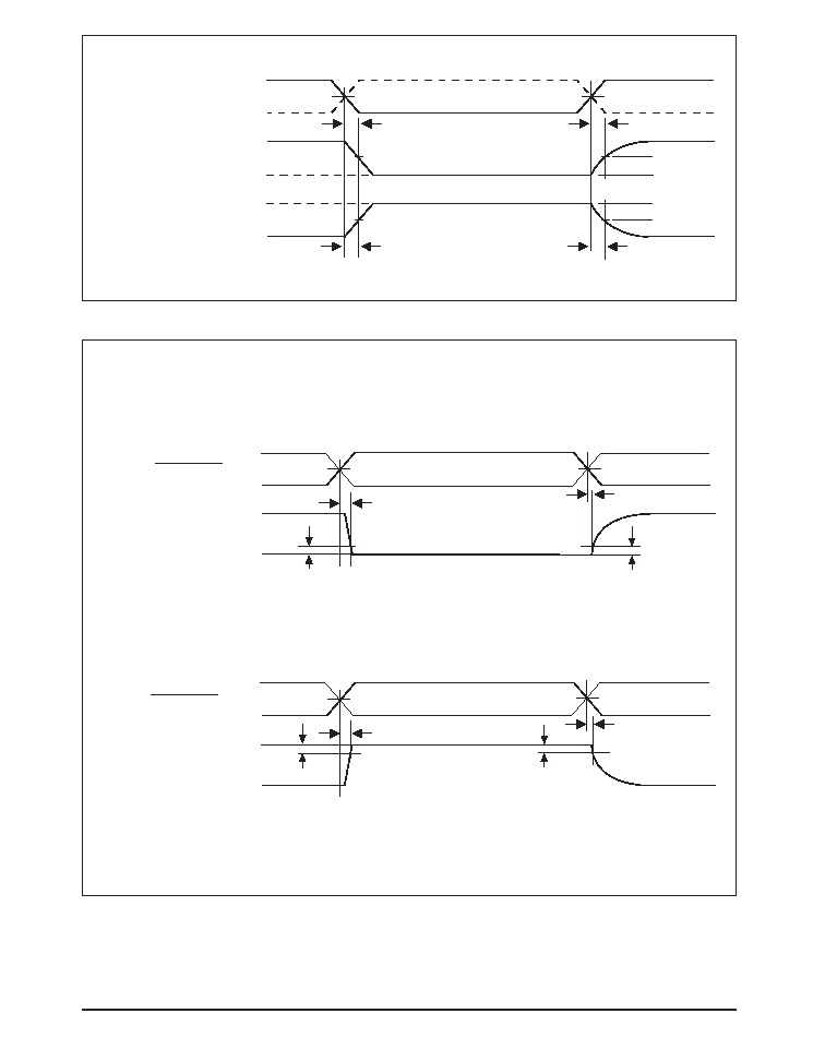
Figure 36. Driver Propagation Delays
Figure 37. Driver Enable and Disable Times
Figure 38. Receiver Propagation Delays
+3V
0V
5V
V
OL
A, B
0V
1.5V
1.5V
t
ZL
t
ZH
V
OH
A, B
2.3V
2.3V
t
LZ
t
HZ
0.5V
0.5V
Output normally LOW
Output normally HIGH
DECx or Tx_Enable
V
OH
V
OL
RECEIVER OUT
(V
OH
- V
OL
)/2
(V
OH
- V
OL
)/2
t
PLH
f > 10MHz; t
R
< 10ns; t
F
< 10ns
OUTPUT
V
0D2
+
V
0D2
≠
A ≠ B
0V
0V
t
PHL
INPUT
t
SKEW
= | t
PHL
- t
PLH
|
+3V
0V
A
B
DRIVER
OUTPUT
V
O
+
DIFFERENTIAL
OUTPUT
V
A
≠ V
B
0V
V
O
≠
1.5V
1.5V
t
PLH
t
R
t
F
f > 10MHz; t
R
< 10ns; t
F
< 10ns
V
O
1/2V
O
1/2V
O
t
PHL
t
DPLH
t
DPHL
t
SKEW =
|
t
DPLH -
t
DPHL
|
DRIVER
INPUT
14
Rev: A Date: 1/27/04
SP506 Multi≠Mode Serial Transceiver
© Copyright 2004 Sipex Corporation
Figure 39. Receiver Enable and Disable Times
Figure 40. V.28 (RS-232) and V.10 (RS-423) Driver Enable and Disable Times
+3V
0V
5V
RECEIVER OUT
0V
1.5V
1.5V
t
ZL
t
ZH
RECEIVER OUT
1.5V
1.5V
t
LZ
t
HZ
0.5V
0.5V
Output normally LOW
Output normally HIGH
V
IL
V
IH
DECx or RCVR Enable
+3V
0V
DECx or Tx_Enable
1.5V
1.5V
t
ZL
T
OUT
t
LZ
Output LOW
0V
+3V
0V
V
OH
1.5V
1.5V
t
ZH
T
OUT
0.5V
t
HZ
Output HIGH
0V
DECx or Tx_Enable
V
OL
0.5V
0.5V
0.5V

15
Rev: A Date: 1/27/04
SP506 Multi≠Mode Serial Transceiver
© Copyright 2004 Sipex Corporation
Figure 41. Typical V.28 Driver Output Waveform
Figure 42. Typical V.10 Driver Output Waveform
Figure 43. Typical V.11 Driver Output Waveforms
Figure 44. Typical V.35 Driver Output Waveforms

16
Rev: A Date: 1/27/04
SP506 Multi≠Mode Serial Transceiver
© Copyright 2004 Sipex Corporation
PINOUT
PIN ASSIGNMENTS
CLOCK AND DATA GROUP
Pin 1 -- RxD -- Receive Data; TTL output,
sourced from RD(a) and RD(b) inputs.
Pin 14 -- TxD -- TTL input ; transmit data
source for SD(a) and SD(b) outputs.
Pin 15 -- TxC -- Transmit Clock; TTL input for
TT driver outputs.
Pin 20 -- RxC -- Receive Clock; TTL output
sourced from RT(a) and RT(b) inputs.
Pin 22 -- ST -- Send Timing; TTL input; source
for ST(a) and ST(b) outputs.
Pin 37 -- RT(a) -- Receive Timing; analog
input, inverted; source for RxC.
Pin 38 -- RT(b) -- Receive Timing; analog
input, non-inverted; source for RxC.
Pin 42 -- ST(a) -- Send Timing; analog output,
inverted; sourced from ST.
Pin 44 -- ST(b) -- Send Timing; analog output,
non-inverted; sourced from ST.
Pin 59 -- SD(b) -- Analog Out -- Send data,
non-inverted; sourced from TxD.
Pin 61 -- SD(a) -- Analog Out -- Send data,
inverted; sourced from TxD.
Pin 63 -- TT(a) -- Analog Out -- Terminal
Timing, inverted; sourced from TxC
Pin 65 -- TT(b) -- Analog Out -- Terminal
Timing, non≠inverted; sourced from TxC.
Pin 70 -- RD(a) -- Receive Data, analog input;
inverted; source for RxD.
Pin 71 -- RD(b) -- Receive Data; analog input;
non-inverted; source for RxD.
Pin 76 -- SCT(a) -- Serial Clock Transmit;
analog input, inverted; source for SCT.
Pin 77 -- SCT(b) -- Serial Clock Transmit:
analog input, non≠inverted; source for SCT
Pin 79 -- SCT -- Serial Clock Transmit; TTL
output; sources from SCT(a) and SCT(b) inputs.
CONTROL LINE GROUP
Pin 13 -- DTR -- Data Terminal Ready; TTL
input; source for TR(a) and TR(b) outputs.
Pin 16 -- RTS -- Ready To Send; TTL input;
source for RS(a) and RS(b) outputs.
Pin 17 -- RL -- Remote Loopback; TTL input;
source for RL(a) and RL(b) outputs.
Pin 19 -- DCD-- Data Carrier Detect; TTL
output; sourced from RR(a) and RR(b) inputs.
Pin 21 -- RI -- Ring In; TTL output; sourced
from IC(a) and IC(b) inputs.
Pin 24 -- LL -- Local Loopback; TTL input;
source for LL(a) and LL(b) outputs.
Pin 35 -- RR(a)-- Receiver Ready; analog
input, inverted; source for DCD.
Pin 36 -- RR(b)-- Receiver Ready; analog
input, non-inverted; source for DCD.
Pin 39 -- IC(a)-- Incoming Call; analog input,
inverted; source for RI.
Pin 40 -- IC(b)-- Incoming Call; analog
input,non-inverted; source for RI.
RxD 1
SDEN
2
TREN
3
RSEN 4
LLEN
5
TTEN 6
SCTEN 7
LATCH 8
DEC
3
9
DEC
2
10
DEC
1
11
DEC
0
12
DTR 13
TxD 14
TxC 15
RTS 16
RL 17
RLEN 18
DCD 19
RxC 20
RI 21
ST 22
STEN 23
LL 24
V
CC
25
C
1
+
26
V
DD
27
C
2
+
28
GND 29
C
1
≠
30
C
2
≠
31
V
SS
32
V
CC
33
GND 34
RR(a) 35
RR(b) 36
R
T(a) 37
R
T(b) 38
IC(a) 39
IC(b) 40
60 GND
59 SD(b)
58 TR(a)
57 GND
56 TR(b)
55 V
CC
54 RS(a)
53 GND
52 RS(b)
51 LL(a)
50 GND
49 LL(b)
48 V
CC
47 RL(a)
46 GND
45 RL(b)
44 ST(b)
43 GND
42 ST(a)
41 V
CC
80 CTS
79 SCT
78 DSR
77 SCT(b)
76 SCT(a)
75 GND
74
V
CC
73
V
CC
72 GND
71 RD(b)
70 RD(a)
69 DM(b)
68 DM(a)
67 CS(b)
66 CS(a)
65
TT(b)
64 GND
63
TT(a)
62
V
CC
61 SD(a)
SP506

17
Rev: A Date: 1/27/04
SP506 Multi≠Mode Serial Transceiver
© Copyright 2004 Sipex Corporation
Pin 7 -- SCTEN -- Enables SCT receiver;
active high; TTL input.
Pin 8 -- LATCH -- Latch control for decoder
bits (pins 9-12), active low. Logic high input
will make decoder transparent.
Pins 12≠9 -- DEC
0
≠ DEC
3
-- Transmitter and
receiver decode register; configures transmitter
and receiver modes; TTL inputs.
Pin 18 -- RLEN -- Enables RL driver; active
low; TTL input.
Pin 23 -- STEN -- Enables ST driver; active
low; TTL input.
POWER SUPPLIES
Pins 25, 33, 41, 48, 55, 62, 73, 74 -- V
CC
-- +5V
input.
Pins 29, 34, 43, 46, 50, 53, 57, 60, 64, 72, 75 --
GND -- Ground.
Pin 27 -- V
DD
+10V Charge Pump Capacitor --
Connects from V
DD
to V
CC
. Suggested capaci-
tor size is 22µF, 16V.
Pin 32 -- V
SS
≠10V Charge Pump Capacitor --
Connects from ground to V
SS
. Suggested ca-
pacitor size is 22µF, 16V.
Pins 26 and 30 -- C
1
+
and C
1
≠
-- Charge Pump
Capacitor -- Connects from C
1
+
to C
1
≠
.
Suggested capacitor size is 22µF, 16V.
Pins 28 and 31 -- C
2
+
and C
2
≠
-- Charge Pump
Capacitor -- Connects from C
2
+
to C
2
≠
.
Suggested capacitor size is 22µF, 16V.
Pin 45 -- RL(b) -- Remote Loopback; analog
output, non-inverted; sourced from RL.
Pin 47 -- RL(a) -- Remote Loopback; analog
output inverted; sourced from RL.
Pin 49-- LL(b) -- Local Loopback; analog
output, non-inverted; sourced from LL.
Pin 51 -- LL(a) -- Local Loopback; analog
output, inverted; sourced from LL.
Pin 52 -- RS(b) -- Ready To Send; analog
output, non-inverted; sourced from RTS.
Pin 54 -- RS(a) -- Ready To Send; analog
output, inverted; sourced from RTS.
Pin 56 -- TR(b) -- Terminal Ready; analog
output, non-inverted; sourced from DTR.
Pin 58 -- TR(a) -- Terminal Ready; analog
output, inverted; sourced from DTR.
Pin 66 -- CS(a)-- Clear To Send; analog input,
inverted; source for CTS.
Pin 67 -- CS(b)-- Clear To Send; analog input,
non-inverted; source for CTS.
Pin 68 -- DM(a)-- Data Mode; analog input,
inverted; source for DSR.
Pin 69 -- DM(b)-- Data Mode; analog input,
non-inverted; source for DSR
Pin 78 -- DSR-- Data Set Ready; TTL output;
sourced from DM(a), DM(b) inputs.
Pin 80 -- CTS-- Clear To Send; TTL output;
sourced from CS(a) and CS(b) inputs.
CONTROL REGISTERS
Pins 2 -- SDEN -- Enables TxD driver, active
low; TTL input.
Pins 3 -- TREN -- Enables DTR driver, active
low; TTL input.
Pins 4 -- RSEN -- Enables RTS driver, active
low; TTL input.
Pins 5 -- LLEN -- Enables LL driver, active
low; TTL input.
Pin 6 -- TTEN -- Enables TT driver, active
low; TTL input.

18
Rev: A Date: 1/27/04
SP506 Multi≠Mode Serial Transceiver
© Copyright 2004 Sipex Corporation
Table 1. SP506 Driver Decoder Table
Table 2. SP506 Receiver Decoder Table
SP506 Receiver Mode Selection
SP506 Driver Mode Selection
Pin Label
RD(a)
RD(b)
RT(a)
RT(b)
CS(a)
CS(b)
DM(a)
DM(b)
RR(a)
RR(b)
IC(a)
IC(b)
SCT(a)
SCT(b)
Pin Label
Mode:
RS232
V.35
RS422
RS449
EIA530
EIA-530A
V.36
0000
0010
1110
0100
0101
1100
1101
1111
0110
SD(a)
tri-state
V.28
V.35≠
V.11≠
V.11≠
V.11≠
SD(b)
V.35+
V.11+
V.11+
V.11+
TR(a)
tri-state
V.28
V.11≠
V.11≠
V.11≠
V.10
TR(b)
tri-state
tri-state
tri-state
V.11+
V.11+
V.11+
tri-state
RS(a)
tri-state
V.28
V.11≠
V.11≠
V.11≠
RS(b)
tri-state
tri-state
tri-state
V.11+
V.11+
V.11+
RL(a)
tri-state
V.28
V.11≠
V.11≠
V.10
RL(b)
tri-state
tri-state
tri-state
V.11+
V.11+
tri-state
LL(a)
tri-state
V.28
V.11≠
V.11≠
V.10
LL(b)
tri-state
tri-state
tri-state
V.11+
V.11+
tri-state
ST(a)
tri-state
V.28
V.35≠
V.11≠
V.11≠
V.11≠
ST(b)
V.35+
V.11+
V.11+
V.11+
TT(a)
tri-state
V.28
V.35≠
V.11≠
V.11≠
V.11≠
TT(b)
V.35+
V.11+
V.11+
V.11+
tri-state
tri-state
tri-state
tri-state
tri-state
tri-state
V.28
V.28
V.28
V.28
V.11≠
V.11+
V.11≠
V.11+
V.11≠
V.11+
tri-state
V.11≠
V.11+
V.11≠
V.11+
V.10
V.11≠
V.11+
V.11≠
V.11+
V.11≠
V.11+
V.11≠
V.11+
V.11≠
V.11+
V.10
tri-state
V.10
tri-state
V.11≠
V.11+
V.10
tri-state
V.10
tri-state
V.10
tri-state
V.11≠
V.11+
V.11≠
V.11+
Mode:
RS232
V.35
RS422
w/ Term.
RS422
RS449
EIA530
EIA-530A
V.36
0000
0010
1110
0100
0101
1100
1101
1111
0110
V.28
V.35≠
V.11≠
V.11≠
V.11≠
V.35+
V.11+
V.11+
V.11+
V.28
V.11≠
V.11≠
V.11≠
V.11+
V.11+
V.11+
V.28
V.11≠
V.11≠
V.11≠
V.11+
V.11+
V.11+
V.28
V.11≠
V.11≠
V.11+
V.11+
V.28
V.11≠
V.11≠
V.11+
V.11+
V.28
V.11≠
V.11≠
V.11+
V.11+
V.28
V.35≠
V.11≠
V.11≠
V.11≠
V.35+
V.11+
V.11+
V.11+
V.28
V.28
V.28
V.11≠
V.11+
V.11≠
V.11+
V.11≠
V.11+
V.10
V.10
V.10
>10k
to GND
>10k
to GND
>10k
to GND
>10k
to GND
>10k
to GND
>10k
to GND
>10k
to GND
>10k
to GND
>10k
to GND
>10k
to GND
>10k
to GND
>10k
to GND
>10k
to GND
>10k
to GND
>10k
to GND
>10k
to GND
>10k
to GND >12k
to GND
>10k
to GND
>10k
to GND
>10k
to GND
>10k
to GND
>10k
to GND
>10k
to GND
>10k
to GND
>10k
to GND
>10k
to GND
V.11≠
V.11+
V.11≠
V.11+
>10k
to GND
>10k
to GND
V.10
V.10
>10k
to GND
V.10
>10k
to GND
V.10
V.11≠
V.11+
V.11≠
V.11+
V.11≠
V.11+
>10k
to GND
V.10
V.35≠
V.35+
V.28
>10k
to GND
V.11≠
V.11+
3
0
DEC ≠ DEC
3
0
DEC ≠ DEC
120
120
120
RS422
w/ Term.
120
120
120
V.11≠
V.11+
V.11≠
V.11+
120
120
120
V.11≠
V.11+
V.11≠
V.11+
V.11≠
V.11+
120
120
120
V.11≠
V.11+
V.11≠
V.11+
V.11≠
V.11+
120
120
120

19
Rev: A Date: 1/27/04
SP506 Multi≠Mode Serial Transceiver
© Copyright 2004 Sipex Corporation
Figure 45. SP506 Typical Operating Circuit
RD(a) 70
RxD 1
RD(b) 71
RT(a) 37
RxC 20
RT(b) 38
CS(a) 66
CTS 80
CS(b) 67
DM(a) 68
DSR 78
DM (b) 69
RR(a) 35
DCD 19
RR(b) 36
IC(a) 39
RI 21
IC(b) 40
SCT(a) 76
SCT 79
SCTEN 7
SCT(b) 77
14 TxD
61 SD(a)
59 SD(b)
2 SDEN
22 ST
42 ST(a)
44 ST(b)
23 STEN
15 TxC
63 TT(a)
65 TT(b)
6 TTEN
13 DTR
58 TR(a)
56 TR(b)
3 TREN
16 RTS
54 RS(a)
52 RS(b)
4 RSEN
17 RL
47 RL(a)
45 RL(b)
18 RLEN
24 LL
51 LL(a)
49 LL(b)
5 LLEN
22
µ
F
22
µ
F
1N5819
VCC
VDD
C1-
C2-
VSS
C1+
C2+
22
µ
F
+5V
10
µ
F
27
25
26
31
28
30
22
µ
F
32
9
10
11
12
MODE
X
1
0
1
0
RS-422 Mode
Input Word
A
B
Charge Pump
A -- Receiver Tri-State circuitry,
V.11, & V.35 termination
resistor circuitry (RxD,
RxC & SCT).
B -- Driver Tri-State circuitry &
V.35 termination circuitry
(TxD, TxC & ST).
SP506
(SEE PINOUT ASSIGNMENTS FOR GROUND PINS)
8
DECODER LA
TCH
LATCH
(SEE PINOUT FOR V
CC
PINS)
20
Rev: A Date: 1/27/04
SP506 Multi≠Mode Serial Transceiver
© Copyright 2004 Sipex Corporation
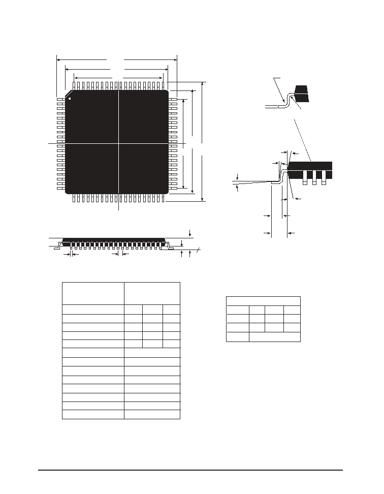
80 PIN MQFP (MS-022 BC)
b
e
Seating
Plane
A1
A
A
L1
5
∞
-16
∞
0
∞
MIN.
0
∞
≠7
∞
5
∞
-16
∞
L
A2
0.30" RAD. TYP.
0.20" RAD. TYP.
c
PIN 1
E1
D1
D
CL
E
CL
D2
E2
DIMENSIONS
Minimum/Maximum
(mm)
SYMBOL
A
A1
A2
b
D
D1
D2
E
E1
E2
e
N
80≠PIN MQFP
JEDEC MS-22
(BEC) Variation
MIN
NOM
MAX
2.45
0.00
0.25
1.80
2.00
2.20
0.22
0.40
17.20 BSC
14.00 BSC
12.35 REF
17.20 BSC
14.00 BSC
12.35 REF
0.65 BSC
80
COMMON DIMENTIONS
SYMBL MIN
NOM
MAX
c
0.11
23.00
L
0.73
0.88
1.03
L1
1.60 BASIC
PACKAGE: 80 PIN MQFP
21
Rev: A Date: 1/27/04
SP506 Multi≠Mode Serial Transceiver
© Copyright 2004 Sipex Corporation
ORDERING INFORMATION
Model
Temperature Range
Package Types
SP506CF ........................................................................... 0∞C to +70∞C ...................................................... 80≠pin JEDEC (BE-2 Outline) MQFP
Sipex Corporation reserves the right to make changes to any products described herein. Sipex does not assume any liability arising out of the
application or use of any product or circuit described hereing; neither does it convey any license under its patent rights nor the rights of others.
Please consult the factory for pricing and availability on a Tape-On-Reel option.
DATE
REVISION
DESCRIPTION
1/27/04
A
Implemented tracking revision.
REVISION HISTORY